 HOME >연구내용 >핵심과제1
2-3. The synthesis and multi scale patterning development of graphene based nano materials for solution-process
| Participants
|
|
||||||||||||||||||||||||
| Research Purpose
Development of high-performance flexible devices based on a single-crystalline silicon for soft electronic devices with high performance which cannot be demonstrated by organic materials, and development of the optimized structure for strain-free flexible device resulting in high performance Si device and circuit with high flexibility
| Contents
Topic 1. Development of transfer process for flexible silicon device and analysis of flexibility
- Development of transfer process for flexible single-crystalline silicon: Bottom Si etching of SOI (silicon-on-insulator) wafer and transfer onto a plastic film
- Strain analysis of the transferred silicon membrane: Analysis of electrical property with bending strain and simulation analysis
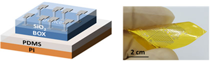
Schematic diagram and photograph of the transferred silicon membrane on PDMS/PI film
Topic 2. Development of ultra-flexible high performance FDSOI transistor
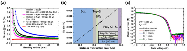
(a) Strain-free structure through optimizing neutral mechanical plane (b) Strain simulation of proposed structure (c) Device characteristics without performance degradation at 1 mm bending Textile form
Topic 3. Gate dielectric formation for soft electronic device by using iCVD
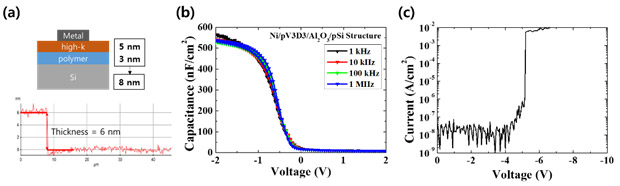
(a) 단결정 실리콘 위에 형성된 High-k/polymer 이중층 구조와 AFM으로 측정한 실제 두께 (b) Capacitance-Voltage 특성 (c) Current-Voltage 특성
| Expected Contribution
| Representative Research Achievement